

An RCD snubber capacitor in a flyback converter must absorb leakage-inductance energy, keep the MOSFET drain spike inside a safe clamp target, survive repetitive pulse current, and fit the physical loop that creates the stress.
When the MOSFET turns off, transformer leakage inductance cannot transfer its stored energy to the secondary. That energy charges the RCD snubber capacitor through the diode and creates the clamp voltage above reflected output voltage. Estimate leakage inductance and worst-case primary peak current first, then decide the acceptable clamp voltage.
SMILER capacitor supplies snubber capacitor products built with metallized polypropylene film, resin filling rated UL94 V-0, and packages intended for high-pulse switching use. Our snubber portfolio is relevant when the design needs a film part instead of a general-purpose capacitor.
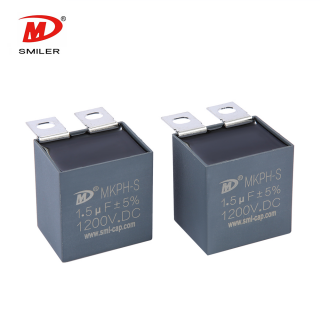
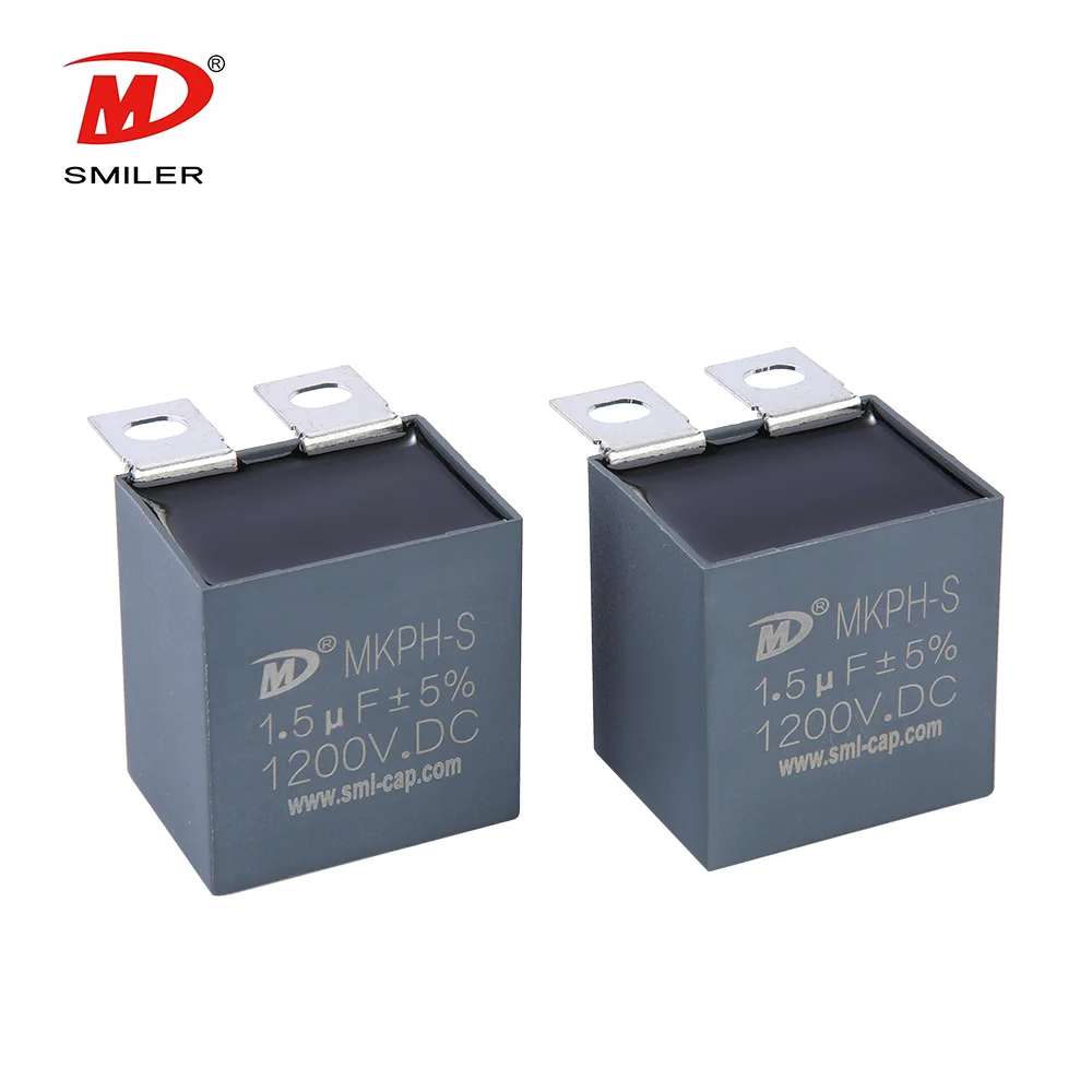
The first filter is the capacitance window. If the calculated RCD snubber capacitor value is small and pulse current is light, compact high-frequency options may work. If the design repeatedly stores measurable leakage energy, check the part as a pulse component. For example, the Power Capacitor Snubber Capacitor MKPH-S uses metallized polypropylene film, a plastic shell package, and resin filling, and the approved feature set includes high pulse intensity, self-healing behavior, flame retardant ability, high reliability, and long useful life.
Leakage energy per switching event is normally estimated from transformer leakage inductance and primary peak current at the worst operating point. Use measured leakage inductance when possible, because winding arrangement and tolerance can shift the number. Stored leakage energy is proportional to leakage inductance and to the square of peak current.
After estimating energy, compare it with repetitive pulse duty rather than a one-time surge. High line, full load, startup, or transient load can apply repeated charge pulses to the clamp capacitor.
Select the clamp target below the MOSFET drain-source voltage rating after allowing margin for maximum input voltage, reflected output voltage, ringing, tolerances, and measurement uncertainty. Lower clamp voltage reduces MOSFET stress but increases snubber dissipation.
Choose clamp ripple, resistor discharge target, and switching frequency as one system.
Once leakage energy, switching frequency, and allowable clamp ripple are known, choose capacitance that limits voltage rise during each turn-off event. If the capacitor is too small, ripple and ringing may still push the MOSFET close to its limit. If it is too large, resistor heating, discharge time, and efficiency can worsen.
The MKPH-S range gives engineers a practical reference window for higher-energy snubber designs: the approved range is 700-3000 VDC with capacitance from 0.047 uF to 6.8 uF, tolerance options of +/-5% or +/-10%, and maximum peak current expressed as IP = C*dV/dT.
Voltage rating is repetitive operating stress, not just a number above nominal clamp voltage. The capacitor sees fast charging edges, and dV/dt converts directly into peak current through I = C*dV/dT. A design that looks acceptable by voltage alone can still overload the capacitor if edge rate is too high.
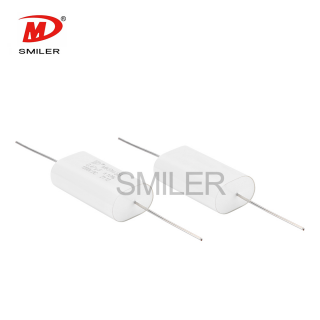
For compact snubber layouts, the Power Capacitor Snubber Capacitor MKPH-LS is an official product option with metallized polypropylene film, plastic-shell or Mylar-tape housing, resin filling rated UL94 V-0, and tinned-copper terminals. Its approved features include low self-inductance, low equivalent series resistance, heat dissipation, and strong ability for withstanding current impact.
The next stress group is thermal. ESR turns pulse current into heat, ESL contributes to residual ringing, and poor heat removal can shorten service life. Check resistor temperature and capacitor case temperature together.
MKPH-LS is specified with a 700-3000 VDC voltage range, +/-5% or +/-10% capacitance tolerance, a -40 C lower category temperature, operation up to +85 C, and a terminal-to-terminal DC test voltage of 1.5 times rated voltage for 10 seconds. Use those ratings as screening data, then confirm waveform and temperature rise.
If the calculated RCD snubber capacitor value is low and energy per cycle is modest, selection may prioritize compact size, low parasitic inductance, and high-frequency stability. A small capacitor placed far from the diode and MOSFET can perform worse than a slightly larger part in a tight loop.
Check capacitance tolerance. A +/-10% part can move clamp ripple and resistor discharge balance in a tight design.
Higher leakage energy, higher switching frequency, or a lower clamp-voltage target pushes the design toward a capacitor built for repetitive pulse duty. Metallized polypropylene film is often selected here because it can combine self-healing behavior, low loss, and pulse-current capability.
SMILER capacitor has more than 15 years of film capacitor expertise, supports customization with low MOQ, and uses automated production lines intended for efficiency, precision, consistency, and quality control. For designers comparing snubber products with broader capacitor categories, the official SMILER capacitor product listing separates snubber capacitors from DC-Link, AC-Filter, CBB, and other capacitor families.
A good RCD snubber capacitor cannot compensate for a long, inductive clamp loop. Keep the MOSFET drain, snubber diode, capacitor, and return path short and direct. Place the resistor so it dissipates heat without warming the capacitor.
Judge capacitor performance after the layout is credible. Excess residual ringing may come from loop inductance, diode recovery, transformer construction, or probe setup.
Base the final BOM decision on measurements across the converter envelope. Check the MOSFET drain waveform, clamp ripple, snubber resistor temperature, capacitor case temperature, and any audible or EMI symptoms. If the resistor overheats, the clamp target or discharge time may be wrong.
Measure VDS at maximum input voltage, full load, startup, output short recovery where applicable, and fast load changes. The peak must remain below the MOSFET limit with real measurement margin.
Confirm that clamp ripple matches the design assumption, residual ringing is acceptable, the resistor has thermal margin, and the capacitor remains within its temperature limit.
A: Estimate leakage energy from leakage inductance and worst-case primary peak current, choose a safe clamp target, define allowable ripple, then select capacitance from that energy and switching frequency. Verify the result on the drain waveform.
A: It should exceed repetitive clamp stress with margin for high line, reflected output voltage, ripple, ringing, tolerance, and temperature derating. Do not size it only from nominal input voltage.
A: It may reduce clamp ripple, but it can increase loss, slow discharge through the resistor, worsen startup stress, raise resistor heating, and reduce efficiency.
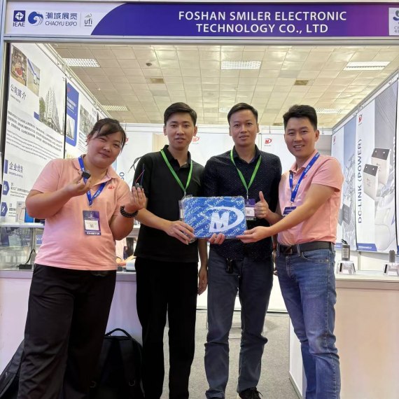
2024 VIETNAM INTERNATIONAL ELECTRONICS & SMART APPLIANCES EXPO
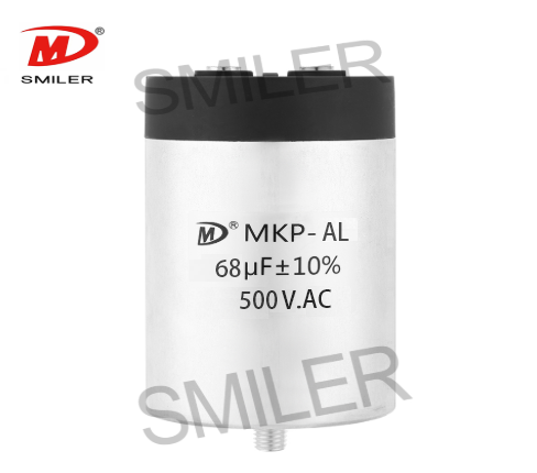
Exploring How AC Capacitors and DC Capacitors Function Differently
Understanding Snubber Capacitor: RC vs. RCD Snubber Differences
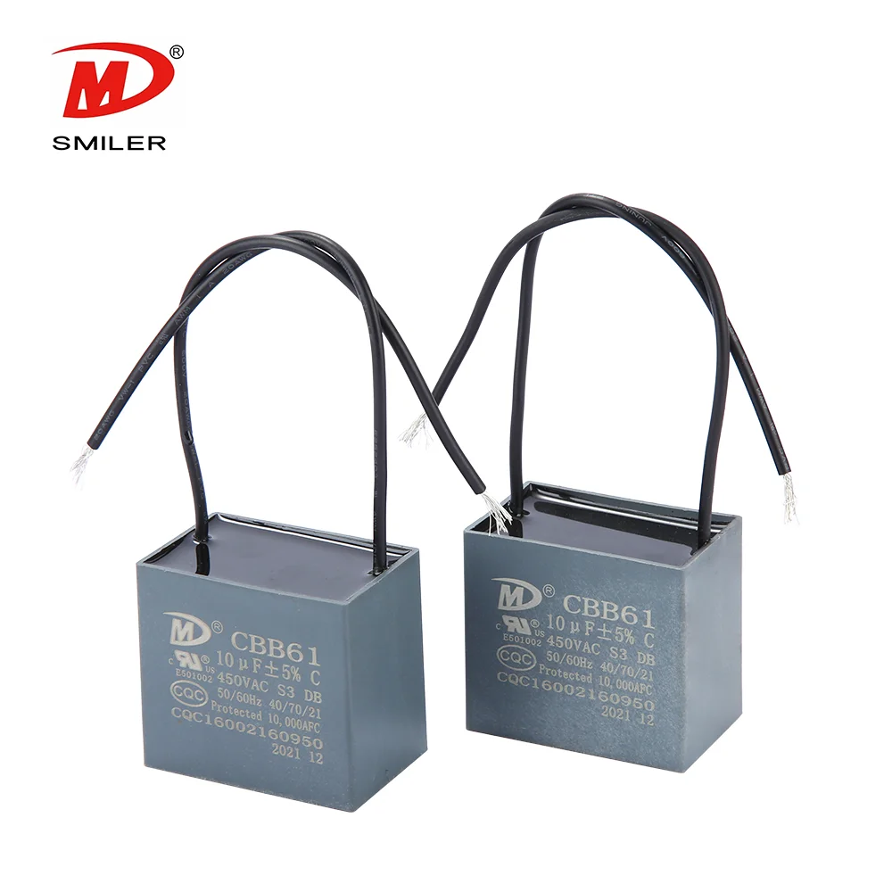
What Does a CBB61 Fan Capacitor Do? Exploring the Role of CBB61 Fan Capacitors
Mastering AC to DC Rectifier with Capacitor Techniques


 Add
Building 12,Huazhi Technology Innovation Center,28 Sanle East Road,Beijiao,Foshan,Guangdong,China
Add
Building 12,Huazhi Technology Innovation Center,28 Sanle East Road,Beijiao,Foshan,Guangdong,China
 Phone
+86 18007576965 / 0757-22391591
Phone
+86 18007576965 / 0757-22391591
 Email
ari@sml-cap.cn
Email
ari@sml-cap.cn



